Electroplating Engineers of Japan Launches Ultra-compact Plating Laboratory Equipment
 TOKYO, July 15, 2015 – Tanaka Holdings Co., Ltd. today announced that Electroplating Engineers of Japan, Limited (EEJA), which operates the Tanaka Precious Metals’ plating business, has developed, and launched from July 15, the RAD-Plater cup-type[1] ultra-compact plating laboratory equipment for semiconductor wafers, which achieves equivalent films to mass-production machines.
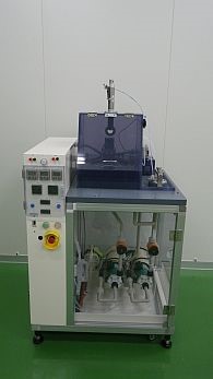
The RAD-Plater is ultra-compact laboratory equipment for manufacturing 2 to 8 inch semiconductor wafers. Measuring 800 mm wide and 700 mm deep, it is smaller than mass production machines and can operate on only compressed air and the 100 volt power of general equipment.
In addition to gold, silver, palladium, copper and nickel, it can use a wide variety of plating solutions including alloys and lead-free solutions, and at 10 liters or less of solution, it uses about half the plating solution required by dip-type machines, which also reduces experimentation costs. The RAD-Plater uses an EEJA-manufactured Stir Cup[2] and delivers mass-production level plating quality through uniform and bubble-less film thickness and superior filling of deep vias[3].
It also enables reduced plating time by using a high current density[4] achieved with an increased ion supply. Even though the RAD-Plater is laboratory equipment, it achieves a level of plating equivalent to that of mass-production machines, which enables early problem-solving in the development stage for mass production issues such as expected yield, and enables trouble-free rollout to the mass-production line. This is the world’s first cup-type plating laboratory equipment for manufacturing semiconductor wafers, using 10 liters or less of plating solution and handling 8-inch wafers.
Many development divisions of manufacturers with mass-production plating lines would have previously contracted out the plating solution experimentation work to equipment manufacturers and others for evaluation, but purchasing a RAD-Plater and conducting experiments in-house now enables a considerable reduction in development lead times. Other customers would have previously purchased mass-production machines to conduct their own experiments, but because the RAD-Plater comes at a cost that is one third to one quarter that of the mass-production machines, they can now achieve considerable cost reductions.
EEJA provides samples of plating solution together with the RAD-Plater to research, development and trial manufacture divisions of manufacturers, universities and other education and research institutes, material manufacturers and others to improve sales of plating equipment and plating solutions for mass production. It aims to achieve RAD-Plater sales of 500 million yen per year by 2017.
Tanaka Precious Metals will be exhibiting at SEMICON West 2015 from July 14th to July 16th at the Moscone Center in San Francisco. Our engineers will be available to answer questions anytime at Booth No. 1628, South Hall.
[1] Cup-type
A specification of equipment for manufacturing semiconductor wafers, using a jet stream of plating solution and agitation to form a film. Another method is dip-type, which immerses the material to be plated. The trend in current plating processes is to use cup-type equipment for wafers of up to 8 inches and dip-type equipment for wafers of 12 inches or greater.
[2] Stir Cup
Random agitation of the solution on the plating surface of wafers improves ion supply uniformity and film thickness uniformity. It also produces pressure differentials in holes in the plating surface to continuously replenish the solution, which prevents bubbles from sticking to the plating surface and improves bubble removal.
[3] Via
A fine through-hole on a wafer or glass substrate to connect metal electrodes on the top and bottom layers of a chip, used as a miniaturization technology for semiconductor chips. Via diameters have recently become smaller, at around 10 to 20 micrometers, making it difficult for conventional plating cups to plate (fill) the inside of the vias with metal.
[4] Current density
Current density has been increased to 1.6 A/dcm2 from the 0.4 A/dcm2 of conventional laboratory equipment.


